

Noticias
Nikon's New APM-3000 Series Fills Gap Between CD SEM and OCD Semiconductor Inspection Devices
jul 15, 2008
Novel CD Inspection Technology Detects Variations in Wafers to Improve Yield
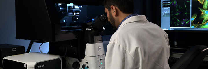
As the advanced IC device process continues to shrink, monitoring pattern profiles has become so critical that Nikon Instruments Inc. launched the APM-3000 Series, an automated pattern profile inspection device that fills the gap between micro and macro semiconductor inspection devices. The APM-3000 Series with Novel CD Inspection Technology leverages a form of birefringence in a Fourier Space to detect Critical Dimension (CD) and Pattern Edge Roughness (PER) variations, ultimately increasing yield rate. Traditional metrology methods, such as CD SEM and OCD has been used for such measurements, but proved timely and potentially damaging to the semiconductors.
The APM-3000 Series compensates for CD SEM and OCD's technical limitations in under half pitch 55 nm. It consists of an optical system with a polarizer and a high NA objective and detects light intensity in a Fourier space. The detecting principal is a form of birefringence of the wafer. With this principle, the CD and PER variations are detected as a polarization fluctuation and converted into the light intensity by use of the polarizer.
"Reports show that electrical abnormality caused by pattern profile- related defects accounts for as much as 65 percent of the reasons for lower yield rates," said Mike Metzger, General Manager, Sales and Marketing, Nikon Instruments. "With the APM-3000 Series, Nikon has created a technology that quickly detects differences between non-defective wafers and wafers with CD defects, helping companies improve yield."
CD SEM monitors the pattern profile with extremely high resolution and measures CD values more accurately than optical microscopes. However, it can damage wafers and hardly detects random fluctuations of the pattern profile occurring in short range. OCD, on the other hand, measures line width, height, depth, wall angle, etc. of the pattern profile by analyzing scattered light. However, it requires significant amounts of simulated data for comparison with measurement data and takes a very long time. Conversely, the APM-3000 Series uses a white LED to minimize damage to the resist. It is able to inspect a wide field of up to . 140 um and has high throughput. Other benefits include quick and easy recipe set-up, high sensitivity with excellent correlation with SEM and quick feedback to the exposure system or SEM review.