Notizie
Nikon Instruments Opens Popular Vote for This Year's Nikon Small World Competition
set 18, 2008
For the second consecutive year, Nikon Instruments is opening up its Small World Photomicrography Competition for the public to choose its favorite image for recognition as the Popular Vote winner. Visitors to http://www.nikonsmallworld.com... have until 5:00 pm EDT on Friday…
Nikon Instruments Launches Online Game With Winning Small World Images
set 16, 2008
Nikon Instruments is giving the public the chance to test its skills and interact with microscopic images typically only viewed by scientists with its new online game, "Identify the Image." The game gives players a series of five 2008 Nikon…
Nikon Introduces Inverted Materials Microscope, Eclipse MA200
set 10, 2008
Nikon Instruments, Inc. introduces the Eclipse MA200, an inverted materials microscope with an innovative design that has been optimized for digital imaging and ergonomic efficiency. The MA200 uses integrated intelligence to automatically combine captured images with data on their observation…
New Digital CAD Overlay Brings Easy Visualization to Nikon's iNexiv VMA Automeasure Software
set 8, 2008
Nikon Instruments, Inc. added a new feature to its iNexiv VMA Automeasure software, the new Digital CAD Overlay, which allows users to easily compare an actual part to its CAD design specification. Eliminating the need for custom overlays or the…
Nikon's New Wafer Loader NWL200 Series Is the First Ever Capable of Loading Wafers as Thin as 100 Micrometers
lug 15, 2008
Accommodating a changing semiconductor manufacturing process where wafers continue to grow thinner, Nikon Instruments Inc., announced its new wafer loader NWL200 Series, the first line-up of wafer loaders capable of loading wafers as thin as 100 micrometers. Using a new…
Nikon's New APM-3000 Series Fills Gap Between CD SEM and OCD Semiconductor Inspection Devices
lug 15, 2008
As the advanced IC device process continues to shrink, monitoring pattern profiles has become so critical that Nikon Instruments Inc. launched the APM-3000 Series, an automated pattern profile inspection device that fills the gap between micro and macro semiconductor inspection…
Nikon's New WES-3000 Wafer Edge Inspection Tool Offers High-Throughput, In-Line Inspection With High-Resolution
lug 15, 2008
Nikon Instruments Inc. announced its new WES-3000 Wafer Edge Inspection Tool, designed to identify defects often experienced with immersion lithography as well as other IC manufacturing processes. The WES-3000 incorporates high-throughput, in-line inspection with a review station featuring high-resolution and…
Nikon Instruments Introduces New Microscopes and Illumination Stand for Education and OEM Markets
lug 15, 2008
Nikon Instruments Inc. announced its new SMZ-445/460 stereoscopic zoom microscopes, combining a very small size with high performance at a low cost for the Industrial and OEM markets. These microscopes allow observation of a wide range of applications, from routine…
Nikon Instruments Introduces LV-DAF for Full System Integration with Eclipse LV Microscope Series
lug 15, 2008
Nikon Instruments Inc. announced its new Dynamic Auto-Focus unit, the LV-DAF, bringing fast, versatile auto-focus to the Eclipse LV semiconductor inspection microscope series and OEM applications. Featuring the newly developed Hybrid Auto-Focus system, the LV-DAF offers a large focus range…
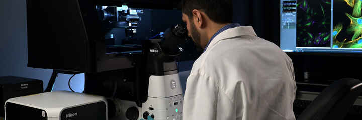
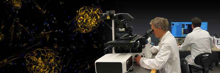
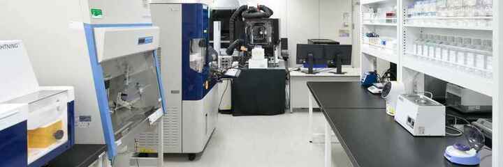
Nikon Instruments Opens New Imaging Center at Northwestern University
giu 4, 2008
Nikon Instruments Inc. and Northwestern University's Feinberg School of Medicine announced the opening of a collaborative core microscopy imaging center, establishing a partnership that brings improved research capabilities to Northwestern, while providing critical feedback for Nikon product development. One of…